


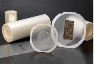
In the semiconductor cutting process, the film is used as a carrier, and different viscosities have different effects on the cutting quality. Using a film with higher viscosity can prevent the die from flying out due to loose adhesion and obtain better cutting quality. However, it will also be difficult to pick up the die due to excessive adhesion. Therefore, choosing the right film during the semiconductor wafer and substrate cutting process is conducive to controlling quality and cost.
Grinding tape is used to protect the circuit surface from damage, chipping, cracks, and contamination caused by foreign matter when grinding the back side of the wafer.
Features of cutting film
1. Applicable to cutting hard and brittle materials such as semiconductor wafers, packaging substrates, ceramics, glass, etc.
2. Good time stability, followability, and stretchability.
3. Easy to peel off and effectively prevent residual glue.
4. Available in a variety of sizes and specifications, and can also be customized as required.
Features of grinding film:
Applicable to wafer backside grinding.
Good adhesion to the concave and convex surface of the wafer.
Good peelability.
Available in various sizes and can be customized as required.
Tel:0731-84014946 Address:Yuelu District New Changhai Jianshan Science and Technology Park, Changsha, Hunan Website: www.csgqet.com
Copyright © 2024 all right reserved :Changsha Guangqi electronic Technology Co., LTD
备案号:
湘ICP备11111111号

