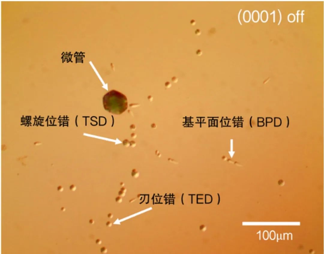
In SIC crystals, there are many defects, and some of them will significantly affect the performance of the device. The main types of defects include macro defects such as microtubules, crystal worlds, multi -type miscellaneous objects, carbon mixed objects, and stacking layer errors (SF), blade position (TED), spiral position (TSD), and base levels wrong. (BPD) and its mixed bit wrong. In terms of density, the quality of SIC crystals has been improved in recent years. Among them, the density of microtubquins is 1 to 10/cm², and the density density is about 10³ to 10⁴/CM². Nevertheless, SIC's defect density is still high compared to SI.
Micro -pipe is considered to be a spiral position with large displacement, and there is empty in the center. Carbon jackets are carbon dust embedded in the process of crystal growth, causing high density or wrong to produce. These defects have a serious impact on the performance of the device.
Figure 1 shows the concave pits formed by the surface of the 8H-SIC substrate on the surface of the 4H-SIC substrate of 8 ° (0001) through the KOH melting. The position of the wrong line extends vertically, and after etching, a hexagonal pit is formed on the surface. In contrast, the base surface is extended parallel to the direction of the (0001) surface, forming an oval pit. There are differences in the shift of the spiral position errors. The spiral bits with a large offset and the mixed bit error will cause the device leakage current, while most small bits error impact on the performance of the device less.
 Figure 1: Through melting KOH, a photo of etching pit on the surface of the SIC substrate
Looking closely at the structure of the base surface, it can be found that it is linear and is surrounded by two shockley parts. When the basal plane is wrong, when the bipolar current passes through the SIC device, it will cause the stack layer to expand, which will cause the degradation of the performance of the device such as resistance.
Figure 2 shows the expansion process of the stacking layer when the bilateral current flows through the SIC device:
The base surface is derived on the SIC substrate and extends to the drift layer.
When the bilateral current flows out, the electrons and holes in the drifting layer are captured by the base surface.
The captured electronics and cavities are released when the energy is released, which prompts some position to move. The movement of the movement of the movement forms a new stacking layer errors. These layers of errors are further captured by electronics and acupoints, resulting in the continuous movement of partial bits, which continues to expand the stacking layer error area. These stacked layers of error areas show high resistance and affect the performance of the device.
In high -concentration N -shaped areas, due to the short complex life of electronics and holes, the cavity density of the buffer layer or the substrate is low, so the expansion of the stacking layer is mainly occurred in the drift layer. In addition, the boundary of the stacking layer is stable (not moving) in crystal science, so the expanded stack layer error area is usually rectangular or triangular.
By optimizing the growth conditions of the extension, the base surface of the drifting layer can be greatly reduced. Today, the appropriate buffer layer has significantly reduced the base surface error density of SIC extension and intermediate drifting layer.
Figure 3: TEM images that form crystal defects due to ion injection
When ion injection, SIC will cause crystal defects. Figure 3 and 4 show the high -concentration AL ion injection and annealing cross -section TEM (transmitted electron microscope) image on SIC. Figure 3 shows the area injected with AL, with high -density black defects, which are caused by crystal deformation. Even after high temperature annealing, the crystal has not fully recovered. Figure 4 enlarged the defective area and displayed high -resolution TEM crystal images. You can observe the 4H-SIC structure with a period of 1 nanometer and a cycle of one cycle. The position of the arrow shows a layer of additional lattice layer, forming a Frank stacking layer. It is reported that the injected AL element is concentrated into a layered structure, resulting in the formation of stacking layer errors.
Figure 4: High -resolution images in the defect
Tel:0731-84014946 Address:Yuelu District New Changhai Jianshan Science and Technology Park, Changsha, Hunan Website: www.csgqet.com
Copyright © 2024 all right reserved :Changsha Guangqi electronic Technology Co., LTD
备案号:
湘ICP备11111111号